




PCB heat dissipation depends on a complete path from heat-generating components to the surrounding environment. Copper planes, thermal vias, and heat sinks can help, but their effectiveness depends on component losses, package construction, solder attachment, and the final enclosure. Improving one part of that path may achieve little when another part remains the bottleneck.
For engineers and technical buyers, overheating is therefore a specification problem as well as a layout problem. A board that operates comfortably on an open bench can behave differently inside a sealed product, beside another heat source, or under sustained load. The practical objective is to keep components within their application-specific temperature limits using a design the fabricator and assembler can reproduce. That starts with a realistic loss estimate and ends with testing under representative operating conditions.
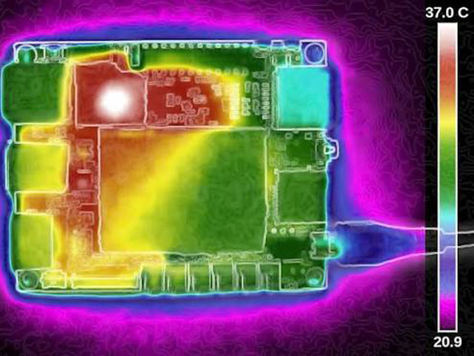
Heat moves through solids by conduction and leaves exposed surfaces through convection and radiation. Depending on the package, a component can transfer heat into the PCB through its exposed pad, terminals, or other connections. The board then spreads that heat toward a larger surface or a designed cooling interface.
Distinguish heat spreading from heat rejection. Spreading heat over more copper can reduce a local hot spot. The product must still transfer that energy to air, a chassis, or another cooler structure. A uniformly warm board may be spreading heat effectively while still lacking sufficient cooling capacity.
STMicroelectronics explains in its AN5036 guidance on host PCB cooling that thermal vias carry heat into internal ground and power planes, which distribute it through the board. Its guidance also recognizes that layer construction depends on the individual design. AN5036
For a design review, identify three things: where the heat originates, how it reaches a spreading surface, and where it finally leaves the product. This helps distinguish a restricted copper path from an enclosure cooling problem before specifying more expensive construction.
A power converter delivering substantial output power does not dissipate all that power inside its controller. Conversely, a small regulator can become a concentrated heat source when its conversion losses are high.
For an illustrative linear regulator, the main dissipation term is approximately:
P_loss ≈ (V_in − V_out) × I_load
A hypothetical conversion from 12 V to 5 V at 0.4 A produces approximately 2.8 W of regulator heat, excluding quiescent and other losses. That is a calculation example, not a tested board result. Whether it is acceptable depends on the package and complete cooling arrangement.
For switching stages, estimate conduction and switching losses using the selected device documentation and operating conditions. Include startup, sustained duty, simultaneous channel loading, and temperature-dependent losses where relevant. Record the assumptions alongside the PCB schematic so a circuit change triggers a thermal review.
Specify the component’s design temperature target, the relevant local ambient condition, and a documented margin below applicable limits. There is no universal safe PCB temperature that covers every semiconductor, connector, capacitor, and laminate.
An illustrative steady-state screening budget is:
R_effective,target ≤ (T_j,target − T_ambient,local) / P_loss
With assumed values of 110°C, 55°C, and 2.8 W, the budget is approximately 19.6°C/W. This is a target for the defined system conditions, not a material property or validated prediction. Nearby heat sources and transient loads require additional analysis.
Texas Instruments’ Semiconductor and IC Package Thermal Metrics explains why datasheet junction-to-ambient resistance, θJA, depends on the test board and environment. Treating it as a fixed property of the package can produce misleading application temperatures. Use it cautiously for screening; obtain stronger evidence from suitable models and measurements. ti.com
If the loss estimate already makes the cooling budget impractical, reconsider efficiency, package choice, or operating requirements before optimizing the footprint. Include that decision in the PCB design brief.
Placement determines whether the available board area can serve the hot components. Keep temperature-sensitive circuits away from concentrated power losses where functional constraints allow. Consider the locations of enclosure contacts and airflow openings before fixing the positions of power stages.
Review the copper path at its narrowest section. A large copper area beyond a slot, clearance gap, or narrow neck may contribute less than its appearance suggests. Review the actual fabricated geometry, including plane splits and antipads, rather than judging the colored copper pour alone.
Thicker copper increases the cross-sectional area available for lateral conduction, but it does not repair every weak thermal connection. Additional layers help only when heat can reach useful copper on those layers and eventually leave the assembly. Ask the fabricator to review heavier copper together with required trace spacing, etching constraints, and stack-up construction.
Electrical requirements still govern connectivity. An exposed pad may be tied to ground, another potential, or a switching node. Never connect it to a convenient plane without checking the component documentation. Enlarging a switching-node copper area can also create an EMC trade-off.
A useful PCB layout review should therefore examine thermal spreading, return paths, isolation clearances, and sensitive routing together. Resolve conflicts with the circuit and mechanical teams while component placement can still change.
Thermal vias provide copper connections between layers. Their value depends on their geometry, placement, and connection to useful spreading areas; a via count alone is an incomplete specification.
Start with the selected package’s current layout recommendations. Then agree with the manufacturer on finished hole dimensions, barrel plating, board thickness, spacing, and whether vias in solderable pads require filling and capping. Solder-mask tenting, resin filling, and copper filling are different constructions and should not be described interchangeably.
Analog Devices’ AN-772 design and manufacturing guide for LFCSP packages shows diminishing thermal returns as via count increases in its package example. The guide also connects thermal performance with exposed-pad attachment and assembly design. Its example dimensions should not become universal rules for unrelated packages. Analog Devices
More thermal vias are not automatically the best use of the manufacturing budget. Once another section of the heat path dominates, additional vias may provide limited benefit. They can also introduce assembly considerations when placed inside a solder land.
Before approving a dense array, ask what thermal improvement the model predicts and what fabrication process the array requires. If an extra via group adds cost while an improved chassis contact addresses the dominant restriction, compare both options using the same boundary conditions.
Choose construction changes according to the heat path that needs improvement. The following comparison provides qualitative selection guidance, not guaranteed temperature reductions.
| Option | When to evaluate it | Main trade-off | What to verify |
|---|---|---|---|
| Revised placement and copper geometry | Hot components have restricted access to spreading area | Board space, routing, and EMC constraints | Electrical connectivity and the complete path to a cooling surface |
| Thermal vias into connected planes | Heat must move between layers near the component | Pad assembly details and drilling constraints | Package guidance, plating, via treatment, and plane connections |
| Heavier copper or revised stack-up | Lateral spreading or current-carrying paths are restrictive | Fabrication cost and fine-feature compatibility | Finished copper requirements and modeled benefit |
| Insulated metal substrate | A compatible circuit needs heat transfer toward a metal base | Routing flexibility and dielectric selection | Insulation performance, thermal resistance, and mounting arrangement |
| Heat sink or chassis coupling | Heat needs a stronger route out of the board or package | Mechanical space, interface control, and assembly work | Contact area, electrical isolation, loading, and interface tolerances |
| Forced airflow | The enclosure can support controlled air exchange | Noise, fan power, contamination, and maintenance | Air path and performance at the installed operating point |
Würth Elektronik’s PCB thermal management guidance describes an insulated metal substrate, or IMS, built with copper, insulation, and a metal carrier for applications such as simple single-layer circuits. The presence of metal does not remove the need to assess the intervening dielectric and the final mounting interface. Würth Elektronik
Avoid choosing materials by a single attractive label. A higher glass-transition temperature describes a different property from thermal conductivity; it does not by itself establish improved cooling. Likewise, a thermal conductivity value without layer thickness and geometry is insufficient for comparing complete constructions.
Use the PCB products enquiry to discuss the required construction, but request confirmation of the actual material, stack-up, and process rather than assuming a particular option is available.
The package-to-board attachment deserves its own review. A suitable board stack-up cannot compensate for an attachment that fails to create the intended thermal connection.
For exposed-pad packages, coordinate land geometry, via treatment, solder paste deposition, and reflow development. AN-772 recommends multiple stencil openings for the thermal paddle in its LFCSP guidance. That package-specific approach illustrates why copying an arbitrary paste pattern is less useful than validating a pattern for the actual component and assembly process. Analog Devices
Define the relevant PCB stencil requirements alongside the footprint. Ask the assembler how hidden joints will be inspected and how process changes will be controlled. Where X-ray inspection is appropriate, agree on the evaluation method and acceptance criteria before production.
Do not impose a universal void percentage without considering the package and application. An inspection result should be interpreted alongside component guidance and thermal validation, rather than treated as a standalone cooling guarantee.
Include these requirements in the PCB assembly scope so quotations cover the intended inspection and process-development work. Otherwise, suppliers may price materially different levels of verification.
A heat sink works only through the thermal connection the assembly actually provides. A package intended to release much of its heat through its underside may need a different arrangement from a package designed for top-side cooling. Confirm the intended interface before reserving mechanical space.
For chassis coupling, document the interface area, gap range, insulation needs, contact pressure, and permitted loading. A nominal drawing gap is insufficient if tolerances can leave the interface barely compressed or place excessive force on components.
Evaluate gap-filling materials in their installed condition. Their thickness, compression, contact quality, and electrical properties matter alongside bulk thermal conductivity. Include the mechanical team in selecting the solution and defining assembly checks.
Air cooling needs the same attention to installed conditions. Define where cool air enters, how it passes the hot components, and where heated air exits. A fan’s free-air rating does not establish the airflow available through the finished enclosure. If continuous operation depends on a fan, define what happens when cooling degrades.
Use analysis to compare design options, then test the assembled product under representative conditions. A simulation result is only as useful as its power-loss inputs, material definitions, contacts, and cooling assumptions.
Build a test matrix that includes:
A PCB prototype should reproduce the thermal construction closely enough to answer the design question. A convenient substitute enclosure or different stack-up can make a successful test difficult to apply to production.
Record electrical loading alongside temperature so a cooler result cannot hide reduced output. Define a stabilization criterion for steady-state tests; use time-resolved measurements for startup and pulsed operation. Compare both hot spots and temperature-sensitive neighboring components.
Thermal imaging measures surface temperature, and reflective surfaces require careful emissivity treatment. Use appropriate contact measurements or device telemetry to cross-check uncertain results. Package surface temperature and semiconductor junction temperature are different quantities.
Where the device documentation supports it, TI describes estimating junction temperature from package-top temperature using ΨJT. ΨJT is a characterization parameter, not a true thermal resistance, and its applicability depends on conditions. Do not substitute θJC into the same calculation without a valid model of the heat path. ti.com
For production release, retain the test setup, firmware operating mode, material revisions, and acceptance results. Reassess thermally significant PCB components substitutions, even when their electrical function appears equivalent.
Give suppliers a defined operating problem and a reproducible construction. “Improve heat dissipation” leaves too much room for incompatible assumptions.
Provide the board outline, fabrication data, proposed stack-up, assembly files, BOM, component documentation, and mechanical drawings. Identify hot components and include the power-loss estimates, temperature targets, operating modes, and environmental conditions that justify the cooling design.
Specify via treatment, copper requirements, interface materials, hidden-joint inspection, and the scope of thermal testing. Distinguish engineering samples from production quantities, and state which design features may change during optimization.
Request separate pricing for meaningful alternatives: copper changes, filled-and-capped vias, revised board materials, interface hardware, or additional validation. Ask each supplier to identify assumptions and exclusions. This makes cost differences understandable and helps prevent a cheaper quotation from silently omitting necessary work.
Agree who approves design changes and what evidence is required before release. The useful deliverable is a board and assembly specification tied to operating limits and test results.
Identify the restrictive part of the heat path first. Improve copper geometry and layer connections when spreading is inadequate; improve enclosure coupling or airflow when heat cannot leave the product. Compare changes under the same operating conditions.
There is no universal count. Start with the component manufacturer’s recommendations, then consider power loss, via construction, board thickness, and connected copper. Confirm the array with the fabricator and assembler, and validate its benefit through analysis or testing.
No. An appropriate metal-base construction can improve heat transfer, but its dielectric, mounting interface, and available cooling surface still matter. Compare complete assemblies that meet the same electrical, mechanical, and routing requirements.
Sometimes improved spreading is sufficient, but heavier copper cannot guarantee adequate heat rejection. The answer depends on losses, board area, enclosure conditions, and temperature limits. Test the proposed construction before removing cooling hardware.
No. A thermal camera measures a surface and requires appropriate measurement settings. Junction temperature needs device telemetry or a justified estimation method. A package-top reading can support an estimate when an applicable characterization parameter is available.
Review the exact package, exposed-pad geometry, loss characteristics, temperature ratings, and assembly guidance. Repeat the relevant thermal test when the substitution changes dissipation or heat flow. Electrical interchangeability alone does not establish equivalent thermal performance.


Learn how PCB impedance coupons, TDR measurements, tolerance limits, and traceable reports support fabrication acceptance and more accurate supplier RFQs.

Compare flying probe and bed-of-nails for bare multilayer PCBs, including electrical coverage, netlist control, probe access, fixture economics, and RFQ requirements.

Learn the differences between PCB surface preparation, wet processing, and final finishes, with practical guidance on plating terminology, inspection evidence, and RFQ requirements.