




EMC PCB design controls how electromagnetic noise is generated, travels through a product, and affects other circuits or equipment. Grounding establishes return paths, shielding limits field coupling, and filtering reduces unwanted energy on power and signal connections. Their effectiveness depends on how the board, enclosure, cables, and operating modes work together.
For hardware engineers and OEM teams, the practical challenge is choosing which intervention addresses the actual failure mechanism. Adding a shield or filter without understanding that mechanism can increase assembly cost while leaving the problem unresolved. This guide explains how to evaluate grounding, shielding, and filtering as connected design decisions, then translate those decisions into fabrication requirements, prototype tests, and a useful supplier brief. The goal is a design that can be built consistently and evaluated in its intended configuration.
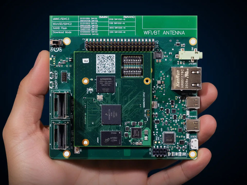
Electromagnetic compatibility has two sides: controlling emissions and maintaining acceptable operation when electromagnetic disturbances reach the product. A board can have low measured emissions yet reset, lose communication, or produce inaccurate readings during an immunity test.
Start the project with an EMC requirements brief. Define the product category, intended markets, installation environment, external interfaces, and intended enclosure. Have the responsible compliance specialist or laboratory identify the applicable standards, editions, test levels, and operating configurations.
Also define acceptable behavior. Is temporary communication loss permitted? Must stored data remain intact? Does an analog measurement have to stay within a specified error band? These questions connect EMC testing to product requirements rather than leaving the laboratory to interpret a functional failure.
Treat EMC performance as a system property. A bare-board electrical test verifies manufacturing connectivity; it does not establish the electromagnetic performance of the assembled product. Supplier responsibilities should state whether the work covers layout review, prototype assembly, diagnostic testing, or coordination with an external laboratory.
A useful EMC review identifies three things: the noise source, the path that carries or couples the noise, and the circuit or external equipment affected.
Potential sources include switching converters, clock drivers, motor interfaces, and rapidly switching digital outputs. Investigate edge transitions as well as repetition frequency: a relatively slow interface can still have fast edges. Distinguish noise circulating in a signal-and-return loop from common-mode current that travels through cables and other unintended system paths.
Texas Instruments’ PCB Design Guidelines For Reduced EMI provides foundational explanations of current loops, differential-mode and common-mode emissions, and cable interfaces. Use those mechanisms to form a testable hypothesis rather than applying every historical layout recommendation universally. ti.com
For an illustrative industrial controller, suppose radiated emissions increase when a sensor cable is attached. That observation makes the cable path worth investigating; it does not prove the sensor circuit generates the noise. Compare operating modes and controlled cable configurations before deciding whether to change the converter layout, connector filtering, or chassis connection.
For many mixed-signal boards, a continuous ground plane with deliberate component placement is a useful starting point. Analog Devices’ guidelines for mixed-signal PCB layout specifically supports a solid single ground plane for systems with one ADC or DAC and low digital current, while recognizing other architectures require different treatment. Analog Devices
At higher frequencies, return current tends to concentrate near the associated signal route over its reference plane. A slot beneath that route can force a detour and enlarge the current loop. Check plane continuity beneath clocks, interfaces, and sensitive connections instead of assuming that a ground net name guarantees a good return path.
Do not split analog and digital ground solely because both labels appear on the schematic. Follow device-specific guidance and examine where current actually flows. Intentional isolation boundaries remain different: preserve the required isolation and use the appropriate isolated interface.
For design review, request an annotated view of critical signals and their reference layers. Ask the reviewer to identify crossings over plane gaps, narrow ground connections, and transitions between reference structures. A visible explanation is more useful than an unqualified statement that the board has “good grounding.”
A layer count alone does not describe an EMC strategy. The stack-up must provide suitable references for critical routes, accommodate power distribution, and remain manufacturable within the approved board construction.
Before routing, agree which layers will carry fast signals and which planes will reference them. Where a signal changes layers, review how its return current transfers between references. Avoid treating additional stitching vias as a universal remedy; their location must serve the relevant path, and isolation boundaries must remain intact.
Review the proposed construction with the PCB design team before layout release. Request the actual layer arrangement, dielectric construction, impedance assumptions, and treatment of critical transitions.
Placement deserves the same attention. Put connector protection and filtering where they can intercept disturbances at the interface. Keep sensitive measurement inputs away from noisy power-stage regions. For switching converters, use the device manufacturer’s layout guidance to identify the rapidly changing current loops; do not assume every high-current connection has the same noise significance.
When reviewing PCB products, confirm the proposed construction directly with the supplier. Additional layers may create better routing options, but approving extra layers without reviewing their use adds cost without establishing a performance benefit.
An EMI filter must attenuate the unwanted disturbance while preserving the wanted signal or supply behavior. Choose the topology after identifying whether the concern is differential-mode noise, common-mode noise, or both.
A ferrite bead’s impedance at a single catalog frequency is insufficient for selection. Analog Devices’ Ferrite Beads Demystified explains that DC bias can reduce suppression performance and that a bead combined with capacitors can produce unwanted resonance. Selection therefore needs impedance-versus-frequency behavior under operating current and an assessment of damping. Analog Devices
For a purchasing specification, identify the approved part and the electrical conditions supporting its selection. Treat an alternative bead as an engineering change requiring review, even if its package and headline impedance match.
For signal-line filters, assess the effect on the interface waveform and timing. A filter that improves an emissions trace but introduces communication errors has not resolved the product requirement.
For a cable interface, establish where the external connection becomes the protected internal circuit. Place the selected filtering and protection around that boundary, and avoid routing untreated conductors alongside the filtered side where coupling can undermine the separation.
Check the filter’s reference connection as carefully as its series element. A shunt component needs an intentional return path; connecting it through a long, inconvenient route can defeat the intended behavior. The appropriate reference may involve circuit ground or chassis, depending on the interface architecture.
Reserve optional footprints only when their installation and bypass states are documented. Otherwise, engineering samples and production builds can accidentally use different configurations.
Shielding is appropriate when field coupling remains significant or when the enclosure must provide a controlled electromagnetic boundary. Its performance depends on seams, openings, penetrations, and electrical connections as well as the shield material.
Murata’s study of PCB ground design and EMI illustrates this dependency. In its simulation, replacing a lower-impedance board-to-metal-plate connection with a 31.6 mm wire increased emissions; at 1 GHz, the result was worse than before the modification. This is a result for that model, not a universal wire-length limit. Murata Manufacturing Co., Ltd.
For a shield can or conductive enclosure, ask how the intended contact will survive assembly and service. Specify contact areas, coating exclusions where applicable, fastening details, and inspection criteria. Confirm that rework can restore the approved configuration.
A defensible cost rule is to investigate the coupling path before adding shielding. Fixing a layout or connection problem can remove the need for extra hardware. Shielding may still be the practical choice when the architecture, enclosure constraints, or remaining coupling justify it. Compare the total cost of each validated solution, including assembly, access, and retesting.
Use this table to prioritize investigation. The observations are diagnostic clues, not proof of a root cause.
| Observation | First investigation | Possible intervention | Trade-off to verify |
|---|---|---|---|
| Emissions change substantially when a cable is connected | Current path through the connector, cable, and enclosure | Interface filtering or revised shield connection | Signal performance and production cable consistency |
| Noise appears near a converter’s operating harmonics | Power-stage layout and coupling into nearby circuits | Placement or routing revision | Thermal performance and board area |
| Analog errors correlate with digital activity | Shared return paths, supply coupling, and placement | Grounding, partitioning, or decoupling changes | Device-specific requirements and routing feasibility |
| A new bead produces a rail-noise peak | Filter impedance under load and interaction with capacitors | Different part or damping arrangement | Voltage drop, load response, and heating |
| Shielding works only with temporary conductive tape | Seams and contact geometry | Repeatable mechanical bond or enclosure change | Assembly effort, serviceability, and inspection |
Plan pre-compliance evaluation around the intended enclosure, cable set, supply, loads, and firmware modes. An exposed development board with a short laboratory cable represents a different configuration from an installed controller with a long harness.
Create a test matrix showing which operating modes exercise each interface and major power load. Include startup, communications activity, and other conditions relevant to the product. Ask the laboratory which configurations provide useful coverage without multiplying tests unnecessarily.
For diagnosis, record the baseline before changing anything. Keep the measurement arrangement consistent and change one variable where practical. Near-field probes can help locate candidate sources, while controlled cable or bonding changes can help investigate propagation paths. Diagnostic improvement still needs confirmation in the relevant emissions or immunity test.
Maintain a short change log linking each modification to its observed result. Include PCB revision, fitted components, firmware, enclosure, cable arrangement, and measurement setup. A successful experiment is much easier to reproduce when the record identifies what was actually tested.
Pre-compliance work should reduce uncertainty before formal evaluation. It does not replace the applicable conformity assessment or guarantee a pass in a different configuration.
A tested prototype is only useful as a production reference when its important details are controlled. During PCB assembly planning, identify approved filter parts, optional-component states, shield installation, and bonding hardware explicitly.
Agree which characteristics require engineering approval before substitution. Relevant examples include suppression components, connector shield arrangements, and enclosure contact materials. Procurement should receive the reason for each restriction so that a sourcing shortage triggers a targeted review rather than an undocumented replacement.
Build inspection should verify the specified construction. It cannot establish RF performance merely by confirming that a contact conducts DC. Likewise, a functional test that exercises communications does not reproduce every EMC disturbance.
Use the supplier’s technology information as a starting point for questions about the proposed build. Request project-specific confirmation of stack-up control, shield assembly, inspection, and traceability. A general capability description should be followed by evidence relevant to the actual design.
A useful RFQ defines the engineering scope and the evidence required for acceptance. For a project involving electronic manufacturing, provide the following information and identify unresolved items:
The next step is a scoped review of the board and its interfaces, followed by a validation plan. Quote accuracy improves when the supplier can distinguish a layout task from an unresolved system-level investigation.
No. EMI describes electromagnetic interference; EMC describes equipment operating acceptably in its electromagnetic environment without creating unacceptable interference. PCB EMC work therefore considers both emissions and susceptibility to disturbances, alongside the complete product configuration.
No. The appropriate arrangement depends on device requirements, current paths, and system architecture. A continuous plane can suit many mixed-signal boards, but intentional isolation and particular converter implementations require their own treatment. Check the actual device guidance.
No. Layer count does not establish return-path quality, interface behavior, enclosure performance, or immunity. Evaluate the actual stack-up and routing, then test the assembled product with its intended cables, supply, loads, and operating modes.
Yes. Interaction with capacitors can create resonance, and operating current can alter a bead’s suppression behavior. Review the complete network under load instead of choosing solely by nominal impedance or assuming more filtering always improves performance.
No. Openings, seams, cable penetrations, and connection impedance affect the result. Evaluate the assembled enclosure and its interfaces. Specify a repeatable contact arrangement rather than relying on a temporary laboratory modification.
No. Emissions testing evaluates disturbances produced by the equipment; immunity testing evaluates its response to applied disturbances. Define the applicable tests and acceptable product behavior separately, including recovery, communication, and measurement requirements where relevant.
Request an initial review before stack-up and placement are fixed, then review critical routing before fabrication. Update the assessment when interfaces, enclosure details, or significant components change. Early review creates more options for controlling cost and layout changes.


Learn how PCB impedance coupons, TDR measurements, tolerance limits, and traceable reports support fabrication acceptance and more accurate supplier RFQs.

Compare flying probe and bed-of-nails for bare multilayer PCBs, including electrical coverage, netlist control, probe access, fixture economics, and RFQ requirements.

Learn the differences between PCB surface preparation, wet processing, and final finishes, with practical guidance on plating terminology, inspection evidence, and RFQ requirements.