




PCB impedance testing checks whether manufactured transmission lines meet an agreed characteristic impedance target. Fabricators commonly use time-domain reflectometry, or TDR, on dedicated test coupons produced alongside the boards. The result helps engineering and purchasing teams verify fabrication quality before committing valuable components to assembly.
A passing number is useful only when its meaning is clear. Does the coupon represent the relevant layer and geometry? Was the differential pair measured in the correct mode? Does the acceptance limit apply to an average or an entire measurement window?
For hardware engineers, quality teams, and OEM buyers, the purchasing decision is therefore broader than choosing a tolerance. The following guidance connects coupon design, measurement conditions, reporting, and supplier approval so that test results become usable acceptance evidence.
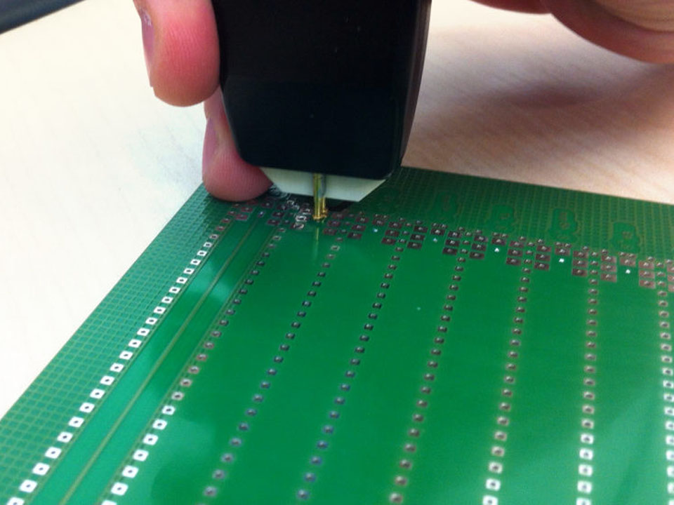
PCB impedance testing verifies the characteristic impedance of a specified transmission-line structure under defined measurement conditions. It does not replace continuity testing or establish that a complete electronic product will function correctly.
Characteristic impedance describes the relationship between voltage and current in a traveling wave. It is different from the DC resistance measured with a multimeter. A trace can have excellent electrical continuity while missing its impedance target.
IPC-TM-650 Method 2.5.5.7, Revision A describes TDR methods for determining PCB transmission-line impedance. A fast voltage step is launched into the structure, and the reflected response is used to calculate impedance. The document also explains that the equipment and measurement procedure affect the result.
Start by identifying which nets need control. The PCB schematic should identify the relevant interfaces and net classes, while the fabrication documentation translates those requirements into layer-specific impedance groups. A general note saying “controlled impedance required” leaves too much interpretation to the supplier.
An impedance coupon is a dedicated test structure made with the production panel. It provides accessible probe locations and a controlled transmission-line geometry without requiring contact with a shippable board’s functional nets.
Polar Instruments’ guidance on testing with coupons explains why coupons reproduce the production layer and trace construction and should represent the panel’s plating, etching, and lamination conditions. Its guidance also illustrates why inaccessible or short product traces can be difficult to measure consistently.
Choose the test according to the question being answered:
| Verification approach | Main question answered | Useful purchasing application | Important limitation |
|---|---|---|---|
| Stackup calculation | Should the proposed construction meet the target? | Engineering review before fabrication | Predicts behavior; does not measure the finished build |
| Coupon TDR measurement | Did the representative manufactured structure meet the agreed limits? | Fabrication acceptance and process monitoring | Does not inspect every routed feature on every board |
| TDR measurement on a product trace | What reflections occur along the accessible product interconnect? | Investigating a specific routing or transition problem | Launches and multiple discontinuities complicate interpretation |
| Channel characterization or interface testing | Does the defined signal path meet its electrical performance requirements? | Product qualification and system validation | Requires a separate scope, fixture strategy, and acceptance criteria |
A coupon offers evidence about the represented construction. Its coverage depends on the coupon design, location, and sampling plan. Testing every panel’s coupons still differs from testing every functional trace on every delivered PCB.
Design the coupon around identifiable impedance groups. A group should distinguish the target, signal layer, reference arrangement, transmission-line structure, and relevant geometry. Two traces with the same nominal target can require different coupon structures when they occupy different layers.
For each group, ask the fabricator to confirm the coupon’s trace width, differential gap where applicable, finished copper thickness, dielectric spacing, and reference-plane arrangement against the approved production construction. Include nearby coplanar copper and solder mask when they form part of the modeled structure.
For a multilayer PCB, overall board thickness alone is insufficient to define a controlled impedance structure. Record the particular dielectric spacing between the signal and its reference conductors. A mechanically acceptable total thickness can coexist with an unsuitable internal distribution of dielectric layers.
Treat coupon artwork as a controlled manufacturing document. If the supplier adjusts production line width after engineering approval, the matching coupon geometry must follow the same approved revision. Otherwise, the test may verify a structure the product does not contain.
Coupon length must support the selected measurement method. A trace that is too short can leave insufficient separation between launch effects and the far-end response. Excessive length can introduce other measurement biases; the test laboratory should approve the usable structure.
Confirm probe-pad compatibility before freezing panel artwork. For stripline structures, also agree how reference conductors are connected within the test coupon. Any temporary connections belong to the approved coupon test arrangement; they do not authorize shorting power and ground on the product board.
Specify the tolerance required by the interface and the design’s validated performance margin, then confirm that the selected construction and supplier can meet it. There is no universal tolerance suitable for every PCB.
Polar’s guide to PCB tolerances describes ±10% as a commonly specified impedance tolerance and discusses tighter ±5% requirements. It also explains that tighter tolerances can increase fabrication cost. These are general industry observations, not a capability commitment from a particular factory or an automatic IPC acceptance rule.
The following arithmetic examples illustrate limits; they are not recommendations for specific interfaces:
| Illustrative target | Specified tolerance | Calculated acceptance interval |
|---|---|---|
| 50 Ω single-ended | ±10% | 45–55 Ω |
| 50 Ω single-ended | ±5% | 47.5–52.5 Ω |
| 100 Ω differential | ±10% | 90–110 Ω |
| 100 Ω differential | ±5% | 95–105 Ω |
A tighter coupon tolerance is useful only when it supports a defined engineering requirement and a credible measurement plan. It cannot compensate for an unsuitable connector launch, excessive channel loss, or a missing return path elsewhere in the design.
Before paying for a tighter limit, ask which failure mechanism it addresses. Request feasibility feedback on the actual layer construction and measurement uncertainty. A catalogue capability statement is weaker evidence than an engineering review of the proposed build.
“100 Ω ±10%” specifies a target and band, but leaves open how the waveform will be judged. State whether acceptance uses an average over an agreed region, an envelope across that region, or another documented rule.
For illustration, a hypothetical trace might average 100 Ω while containing a short excursion outside a 90–110 Ω band. An average-based rule and a whole-window envelope rule can produce different decisions. Agree which applies before production, including how measurement artifacts and rounding are handled.
A single-ended requirement concerns a signal conductor relative to its reference. A differential requirement concerns the two conductors operating as a pair. The report must identify which quantity was measured.
For a symmetric pair, differential impedance equals twice the odd-mode impedance. That relationship does not mean an isolated single-ended measurement can simply be doubled: coupling changes the pair’s behavior. Ask the laboratory to identify its measurement mode and the quantity reported, especially if its software displays both per-conductor and pair values.
Preserve those definitions through PCB layout. Pair gap, signal-to-plane spacing, and nearby copper should follow the approved impedance structure. Separate rules may be needed where a pair changes layers or passes through a connector breakout.
If the supplier proposes changing trace width or gap, require approval for changes that affect design behavior or clearances. The purchaser should explicitly define the fabricator’s adjustment authority rather than assuming that an impedance target overrides every artwork dimension.
A useful test procedure separates the transmission-line response from the measurement setup’s influence. Ask the supplier to define the following conditions before comparing results across laboratories.
Inspect probe contacts and cables, verify calibration status, and check performance against a suitable reference. Polar’s application note on TDR measurement errors identifies worn probes and cables, calibration conditions, and drift as potential error sources. It also shows that fingers or nearby support surfaces can alter surface-trace measurements.
Keep handling and fixture conditions consistent. Repeated measurements that change with probe pressure, cable position, or coupon support call for a setup investigation before concluding that the manufactured trace is unstable.
Define the analysis region after the launch disturbance and before the far-end response contaminates the intended line measurement. Record the region in time or distance and retain the settings used to evaluate it.
Also document the effective rise time and relevant filtering. Changing these settings changes the detail visible in the waveform. A discrepancy between laboratories therefore needs a comparison of settings and launch conditions, not just a comparison of two reported impedance values.
Freeze the approved method for repeated production. A test window should not be moved simply to obtain a passing result; a justified method change needs documentation and approval.
A report should let the buyer connect a result to the delivered hardware and reproduce the acceptance decision. A pass/fail stamp without that context offers limited value during a supplier investigation.
Request the following information as contractual deliverables where appropriate:
For critical groups, request the underlying waveform and sufficient settings to review it. Agree data format and retention period in advance. Screenshots can help investigation, but a screenshot without axes, units, or a defined evaluation region is difficult to assess.
Integrate this evidence into quality control release requirements. If the delivery contains boards from several panels, the inspection records should explain which results support each group of shipped boards.
First establish that the correct structure, target, and test recipe were used. Then separate measurement concerns from manufacturing concerns. This order reduces the risk of changing a good design to compensate for a faulty measurement.
| Observation | Questions to investigate | Evidence to request |
|---|---|---|
| Repeated readings vary on one coupon | Are contact, calibration, cables, and support conditions stable? | Repeated captures using a documented setup |
| One impedance group is consistently outside limits | Does its finished construction match the approved model? | Group-specific artwork, stackup, and dimensional evidence |
| Results differ across a panel | Are coupon locations and local processing conditions representative? | Panel map, coupon locations, and available process records |
| Supplier and customer results disagree | Are mode, launch, window, and processing settings aligned? | A comparison using the same physical coupon and agreed method |
| Coupon passes but a product interface fails | Is the problem in a feature the coupon does not represent? | Investigation of the actual channel and operating conditions |
Cross-sections can support dimensional investigation, but they do not by themselves replace an electrical result. Likewise, a retest should preserve the original failure record and explain why the new result is considered valid.
When production is outside the agreed limits, route disposition through the authorized engineering and quality process. Do not let purchasing pressure turn an undocumented tolerance change into an informal shipment approval.
A uniform coupon does not reproduce every via transition, connector footprint, component pad, or return-path change in a product. It therefore cannot establish complete channel compliance on its own.
For channel validation, assess the signal path that actually exists, including the selected PCB components and their interconnect models where relevant. Define separately whether the project needs frequency-domain characterization, interface compliance testing, or functional testing.
Place coupon acceptance before PCB assembly when the agreed manufacturing flow permits it. This creates a useful release gate before component loading. Retain product-level electrical validation after assembly because fabrication acceptance and assembled-system behavior answer different questions.
Give suppliers a consistent technical package so quotation differences reflect scope rather than assumptions. Coordinate these requirements during PCB design, before the routing and manufacturing data become difficult to revise.
Include:
Cost depends on more than the nominal tolerance. Additional coupon structures consume panel space and test time; extra reporting and laboratory correlation add work. Ask suppliers to price these requirements explicitly instead of comparing a documented verification service with an unspecified “impedance control” option.
For the next RFQ, request written confirmation of the proposed coupon coverage and acceptance method alongside the stackup review. Resolve any exceptions before issuing the production purchase order.
No. A multimeter measures quantities such as DC resistance, not the characteristic impedance seen by a traveling high-speed signal. Use a suitable transmission-line measurement method, commonly TDR, with an appropriate structure and calibrated setup.
Do not assume that a reference to an IPC test method automatically imposes ±10%. Specify the required target and tolerance in the purchasing documents, and identify the applicable acceptance specification and revision separately from the measurement method.
Coverage should represent each distinct controlled structure. The same target on different signal layers can require separate test traces because the construction differs. Several representative structures can share one physical coupon; agree any grouping with engineering before production.
Not necessarily. Acceptance may rely on panel coupons under an agreed sampling and traceability plan. State that coverage explicitly: testing coupons from every panel does not mean every functional trace on every product board was directly measured.
Yes. Differences in calibration, probing, measurement mode, analysis window, and waveform processing can affect the reported value. Compare the same physical coupon using an agreed method before treating the discrepancy as evidence of a fabrication problem.
No. Coupon acceptance supports the represented transmission-line construction. Interface performance also depends on features such as connectors, transitions, components, and operating conditions. Establish a separate channel or system validation plan when the application requires it.


Learn how PCB impedance coupons, TDR measurements, tolerance limits, and traceable reports support fabrication acceptance and more accurate supplier RFQs.

Compare flying probe and bed-of-nails for bare multilayer PCBs, including electrical coverage, netlist control, probe access, fixture economics, and RFQ requirements.

Learn the differences between PCB surface preparation, wet processing, and final finishes, with practical guidance on plating terminology, inspection evidence, and RFQ requirements.