




Effective PCB layout starts before the first trace. Engineers improve routing efficiency by confirming the board stackup, arranging components around real electrical paths, and defining manufacturing constraints before detailed routing begins. These decisions determine whether the remaining work follows a clear plan or becomes repeated placement changes and repair work.
For hardware teams and OEM buyers, efficiency means reaching a board that can be fabricated, assembled, tested, and revised with fewer avoidable surprises. A fully connected layout can still contain an unsuitable return path, an inaccessible programming connector, or a footprint that complicates assembly. The following PCB layout tips connect routing decisions with practical review checkpoints, helping teams judge both the design and the work expected from an external layout partner.
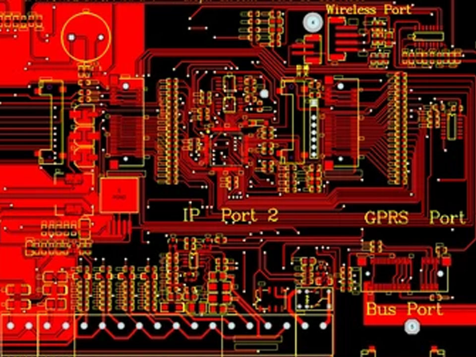
Begin with a reviewed schematic, board outline, enclosure constraints, and proposed manufacturing process. Record which requirements are fixed and which remain open. Connector positions, mounting hardware, component height limits, and isolation boundaries should not emerge after routing is nearly finished.
Create a constraint list for each important circuit: operating current, voltage, interface requirements, reference layers, and any device-specific placement instructions. Check the selected components’ datasheets rather than applying one generic rule to every net. A low-frequency control signal and a fast serial interface may need different treatment even when they share the same voltage.
Altium’s PCB layout guidelines recommend establishing fabrication rules and reviewing the proposed stackup before component placement. Apply that advice by obtaining the intended fabricator’s constraints early and recording the accepted values in the CAD project. Altium
If the circuit definition is still changing, resolve the PCB schematic requirements before requesting a fixed layout quotation. Otherwise, a supplier may price routing work while the customer expects circuit development, component selection, and verification as well.
A PCB stackup defines the copper and dielectric layers available for signals, power, and reference planes. It affects routing space, impedance geometry, and fabrication options. Layer count alone does not describe whether a proposed construction suits the circuit.
For controlled-impedance nets, agree on the layer construction before fixing trace width and spacing. Those dimensions depend on the dielectric geometry, material properties, and copper construction. A width copied from another board is a starting assumption, not a verified solution.
Ask the fabricator which construction is available, how impedance requirements will be communicated, and whether the quoted process includes verification. Keep the approved stackup and routing constraints under the same revision control as the design files.
Additional layers can provide routing capacity or more practical reference-plane placement, but they also affect board cost. Compare complete design alternatives rather than choosing the lowest layer count automatically.
| Design approach | When it deserves consideration | Main trade-off | What to verify |
|---|---|---|---|
| Two-layer construction | Circuits whose routing and return paths can be supported with limited layer resources | Lower construction complexity, but less freedom to preserve copper continuity | Ground connectivity after routing, congestion, and electrical suitability |
| Four-layer construction | Designs needing more routing flexibility and a practical continuous reference plane | Higher board cost than a comparable two-layer construction | Actual layer arrangement, dielectric spacing, and power routing |
| Higher layer count | Dense designs or interfaces requiring additional routing and reference resources | More stackup planning and potentially higher fabrication cost | Escape routing, reference transitions, fabrication process, and validation scope |
These are qualitative planning options, not universal layer-count prescriptions.
Place mechanically fixed components first, then organize the remaining parts by circuit function and connection priority. Treat processor-to-memory connections, sensor inputs, clock circuits, and power stages as interacting groups rather than isolated footprints.
Rotate or reposition devices while examining the unrouted connections. The objective is to create workable routing corridors without violating mechanical, electrical, or assembly needs. A visually neat row of components may create unnecessary crossings; a slightly different arrangement may make the critical connections much easier.
Reserve space for decoupling, termination, and protection components before filling gaps with less constrained parts. Their electrical role often depends on where they connect, so fitting them into leftover space can defeat the intended circuit behavior.
Review package selection alongside placement. Smaller PCB components can reduce occupied area, but their footprints, escape requirements, inspection access, and replacement options may complicate the project. Confirm those trade-offs before shrinking the board outline.
A critical signal route needs a suitable return path as well as a connection between pins. Texas Instruments’ High-Speed Layout Guidelines explain that high-frequency return current follows a low-impedance path near the signal, and that a slot in the reference plane can force a detour and increase loop area. ti.com
Review the reference copper beneath the complete route. Avoid crossing splits or voids that interrupt the intended return path. When a signal changes layers, consider how its return current changes reference layers too; where both references are ground, nearby ground stitching vias may help provide that transition.
Use functional placement to control noise coupling rather than automatically cutting analog and digital ground into separate islands. Any deliberate ground partition needs a circuit-specific justification and a controlled strategy for signals crossing the boundary.
A useful review task is to highlight one critical net, hide unrelated copper, and follow its reference continuously from source to destination. Connectivity checking alone does not establish that this path is electrically suitable.
Route the nets with the least freedom first. Depending on the circuit, these may include memory buses, differential interfaces, clocks, sensitive analog inputs, and power-stage connections. The correct priority comes from the component requirements and circuit architecture.
For differential pair routing, establish the required impedance, spacing, permissible skew, and routing topology from the relevant interface and device documentation. Preserve the intended geometry through the route and review connector breakouts and layer transitions separately.
Length tuning belongs after the basic topology is sound. Adding serpentine routing to a poor path can consume space without resolving its underlying problem. Compare electrical delay where required; equal visible length does not necessarily establish equivalent behavior across different layers or structures.
Leave low-risk connections flexible until constrained routes are proven. If a critical connection requires repeated detours, return to placement rather than treating every routing obstacle as something to solve with another via.
Power routing must satisfy current delivery and the circuit’s noise requirements. Trace width is only one variable: copper thickness, route length, temperature rise, voltage drop, and via transitions also matter. Document the assumptions behind current-carrying geometry instead of relying on a single universal width.
Switching regulator placement requires particular care. Analog Devices’ AN-1119 guidance for step-down regulator layout identifies critical current paths, recommends compact high-current loops, and separates sensitive feedback circuitry from switching nodes. Its examples concern switching controllers; apply the principles alongside the selected regulator’s own instructions. Analog Devices
For a buck converter, identify the rapidly changing current loop rather than treating the entire power section as one equivalent loop. Keep the relevant input bypass path compact, and route feedback from the intended sensing point away from noisy switching copper.
Also inspect narrow sections in copper pours and connections through vias. A wide-looking power region may still contain a bottleneck that determines its resistance or heating. The final review should examine the complete path, including component pads and connectors.
Set rules for manufacturing clearances, copper-to-edge spacing, hole geometry, and any circuit-specific routing requirements. Separate general fabrication limits from electrical constraints such as pair spacing or permitted length mismatch.
A software preset is not always an enforced acceptance limit. The KiCad 9.0 PCB Editor documentation distinguishes preferred routing values from certain minimum and maximum constraints. For example, selecting a preferred differential pair gap in a net class does not, by itself, define the custom limits needed to report a gap violation. KiCad
The broader lesson applies to any CAD workflow: verify what the configured checker actually evaluates. Record exceptions with an owner and engineering reason instead of accumulating unexplained exclusions.
Use interactive routing, saved views, cross-probing, and reusable rules to reduce repetitive work. Review inherited templates before reuse, particularly when the fabricator, stackup, package technology, or product requirements have changed. Automation is most useful when the underlying constraints are correct.
A board can satisfy fabrication constraints and still cause assembly difficulties. Check component courtyards, polarity markings, connector access, and space for the proposed inspection or rework process before approving placement.
Discuss exposed thermal pads and vias within solderable pads with the assembly and fabrication teams. Depending on the construction, the design may require an agreed via treatment and paste strategy. Neither an open via nor a filled via should be assumed appropriate for every package.
Review the PCB stencil requirements alongside the land patterns and paste layers. Aperture decisions should reflect the package, pad geometry, solder paste, and assembly process rather than a blanket reduction applied to every opening.
Provide access for programming, power checks, and the agreed functional tests. Test pads need usable physical access, a defined electrical purpose, and suitable documentation. Review these requirements with the PCB assembly team while placement changes are still manageable.
Routing completion percentage is useful for tracking connectivity, but it should not be the only progress measure. A mostly routed board with unresolved stackup assumptions or test access may be less ready for release than its appearance suggests.
Use three review gates:
This structure also makes outsourced work easier to evaluate. Ask for the decision evidence at each gate rather than accepting screenshots as the sole proof of progress.
For an illustrative example, consider a controller board whose connector moves late in development. The move may alter pair routing, protection placement, enclosure clearance, and test access. Record the change and reopen the affected checks; do not treat it as a purely cosmetic adjustment.
Specify whether the work covers placement and routing only or a broader PCB design scope that includes schematic review, analysis, and manufacturing support. Different scopes create different responsibilities, deliverables, and quotation assumptions.
Prepare the following information for an RFQ:
Ask which inputs remain unresolved and how changes will be handled. A firm delivery date depends partly on timely engineering decisions, not solely on the supplier’s routing capacity.
When commissioning PCB layout, request editable source files and an agreed manufacturing package. Depending on the workflow, that package may include Gerber and drill data or another accepted exchange format, fabrication notes, assembly drawings, placement data, and a revision-matched BOM.
Compare quotations on the same scope. A lower price may exclude library verification, signal-integrity review, mechanical coordination, or support for manufacturing questions. Establish who owns those tasks and what evidence closes each one.
Complete schematic review, verify critical footprints, confirm mechanical constraints, and agree on the stackup and design rules. Placement should demonstrate viable paths for constrained nets. Resolve open interface and manufacturing questions before committing to detailed routing.
Keep unnecessary length under control, but judge each route against its electrical requirements. Reference continuity, impedance, topology, spacing, and timing may matter more than achieving the shortest geometric path. Follow device-specific guidance for constrained connections.
No. Four layers can provide useful routing and reference resources, but suitability depends on the circuit and actual stackup. Compare manufacturability, electrical performance, development effort, and board cost before selecting the construction.
No. Routing automation can help connect nets within configured constraints, but it does not establish that the schematic, footprints, placement, constraints, or test strategy are correct. Engineers still need to review electrical behavior and manufacturing suitability.
Passing DRC shows that the board satisfies the checks that were configured and run. Production readiness also requires schematic agreement, mechanical review, assembly assessment, appropriate electrical verification, and a consistent manufacturing package.
Cost depends on circuit complexity, component density, layer construction, constrained interfaces, library work, review requirements, and input quality. Revision scope and responsibility for analysis or manufacturing support also affect the quotation. Board dimensions alone are an inadequate basis for comparison.


Learn how PCB impedance coupons, TDR measurements, tolerance limits, and traceable reports support fabrication acceptance and more accurate supplier RFQs.

Compare flying probe and bed-of-nails for bare multilayer PCBs, including electrical coverage, netlist control, probe access, fixture economics, and RFQ requirements.

Learn the differences between PCB surface preparation, wet processing, and final finishes, with practical guidance on plating terminology, inspection evidence, and RFQ requirements.